Verfügbarkeit für Abholungen konnte nicht geladen werden
Share
.New Product!Model Number:FPC PCB-0010
Type:FPC
Place of Guangdong,
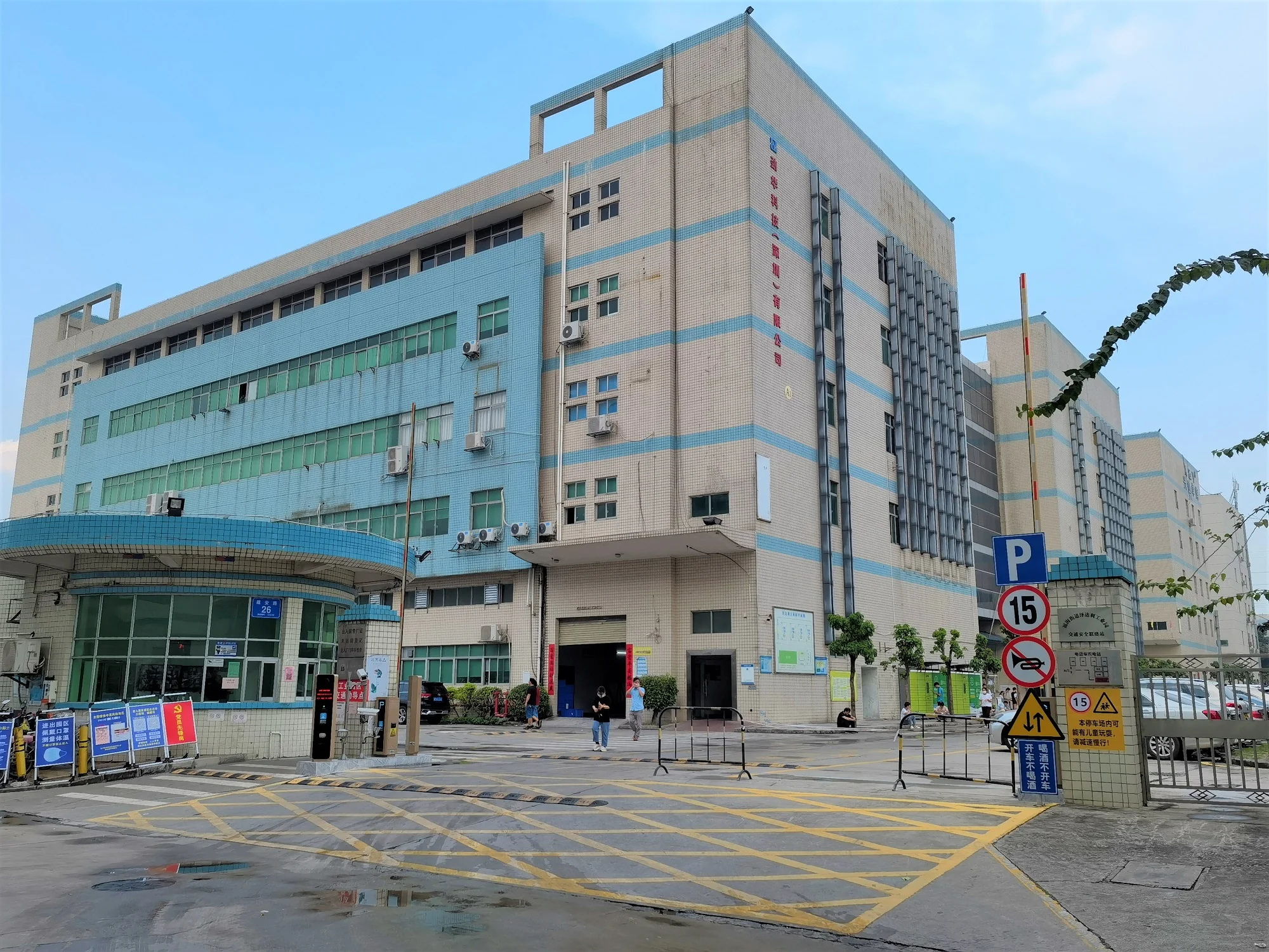
King Field
Base Material:FR4/High TG FR-4/M4/ M6/Rogers/Nelco/Isola
Copper Thickness:1 - 4OZ
Board Thickness:0.2 - 4mm
Min. Hole Size:0.15mm
Min. Line Width:0.1mm
Min. Line Spacing:0.1mm
Surface Finishing:OSP,Immersion Gold,Immersion Tin,Immersion Ag
Board Size:1200*1200mm
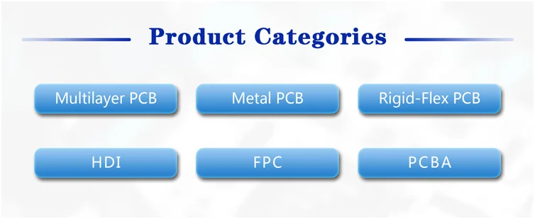
Product name:One-stop PCB Assembly Service
Application:Consumer Electronics
Service:One-stop OEM Service
PCB and PCBA Sample Availability:PCBA Samples
Keyword:FPC Circuit Boards
Certificate:ISO9002/ISO14001/IATF16949
Solder mask color:Green.Black.Red.Yellow.White.Blue.Purple.Matte Green. Matte Black
Assembly Service:SMT Service
Other Service:Assembly
Silkscreen Color:Black.white.yellow.red.blue
Video Description
Company Information
Company introduction
King Field has the capability to manufacture pcb ranging from basic single sided boards up to forty layers, and provide one stop turnkey services, including pcb manufacture, assembly, components sourcing and function testing.With one-stop solution, high-end product structure, professional product development and manufacturing technology, stable quality performance and well management system,
King Field has established long-term and stable cooperate relations with the world's leading communication equipment , aerospace electronics and medical equipment manufacturers.transparent flex PCB FPCB FPC connector Custom Flexible PCB flex board maker
RPCB Main Equipment
FPCB Manufacturing Capability
Item
Production capability
Layer Count
1~6
Production size(Min & Max)
250mm×40mm / 710mm×250mm
Copper thickness of lamination
1/3 ~ 1oz
Product board thickness
0.036 ~ 2.5mm
Auto-cutting accuracy
±0.1mm
Drill size(Min/Max/hole size tolerance)
0.075mm/ 6.5mm / ±0.025mm
Min percent for CNC slot length and width
2:01:00
maximum aspect Ratio (thickness/hole diameter)
8:01
Homogeneity of Plating Cu
≥90%
Accuracy of pattern to pattern
±3mil ( ±0.075mm)
Accuracy of pattern to hole
±4mil ( ±0.1mm )
Min line width/space
0.045 /0.045
Etching tolerance
±20%(±0.02mm)
Cover layer alignment tolerance
±6mil (±0.1 mm)
Excessive adhesive tolerance for pressing C/L
0.1mm
Alignment tolerance for thermosetting S/M and UV S/M
±0.3mm
Min S/M bridge
0.1mm
Min space for S/M to pad, to SMT
0.075mm / 0. 1mm
Min space for legend to pad/ to SMT
0.2mm / 0.2mm
Surface treatment thickness for Ni/Au/Sn/OSP
1~6um /0.05~0.76um /4~20um/ 1um
Min size E- tested pad
8 X 8mil
Min space between tested pads
8mil
Min dimention tolerance of outline (outside edge to circuit)
±0.1mm
Min dimention tolerance of outline
±0.1mm
Min R corner radius of outline (Inner filleted corner)
0.2mm
Min space golden finger to outline
0.075mm
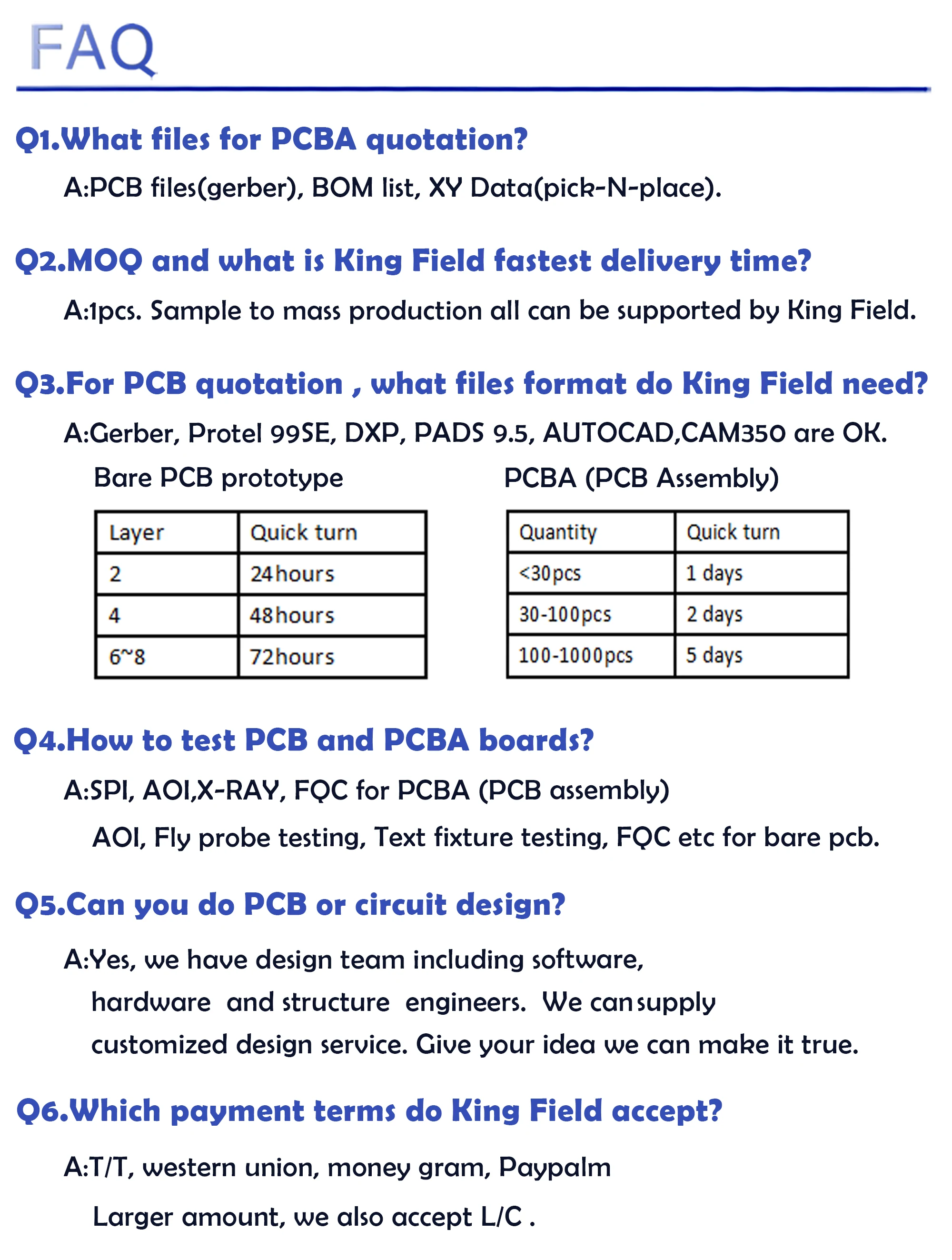
PCB manufacturing
Layer
quick turn
(hours)
usual time
(days)
Mass productions>30m2
(days)
2
24
<4
<10
4
48
<6
<12
6
72
<8
<14
8
96
<10
<16
10
120
<12
<18
Certifications
Product packaging
services we provide
.Hot Product!
.By Hong Kong Yuanfeng Intermational Technology Industry.